FUKUDA has developed copper and copper-based nanoparticles.
Nanoparticles
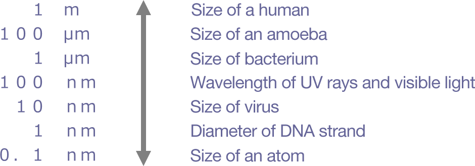
The prefix "nano" means "one billionth." Nanoparticles are considered particles with a diameter smaller than 1 nm (10-9m). One characteristic of nanoparticles, for example, is that when a solid becomes a particle smaller than a few dozen nanometers, then the quantum size effect causes the melting point to drop to near room temperature. That means nanoparticles can exhibit various functional characteristics that are not observed in the bulk state of the same material.
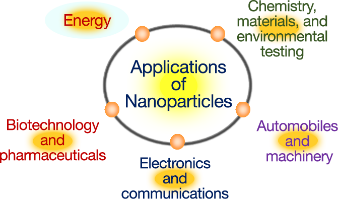
Applications of Nanoparticles
Nanoparticles are used in a wide variety of fields, such as chemicals, materials, pharmaceuticals, and biotechnology, with further technological advances expected in the future. Due to the high conductivity of metal nanoparticles, in particular metals such as gold, silver, and copper, they are being actively researched for use in forming fine wiring patterns in electronic parts. Metal nanoparticles are also expected to be used in making highly efficient thermally conductive materials, due to their high thermal conductivity, or to be used in highly active catalysts, due to their high specific surface area, for example.
Using Copper and Copper-Based Nanoparticles for Printed Electronics
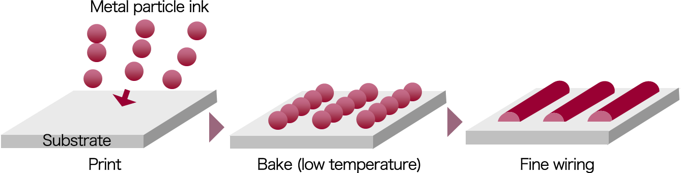
There is growing interest in a technology called printed electronics, a next-generation wiring technology that is essential for advancements in electronic fields, such as for smartphones, electronic paper, and digital signage. Unlike conventional technologies for forming wiring patterns based on photolithography, it involves printing technologies, such as inkjet or screen printing, to print wiring patterns directly onto a substrate, using conductive inks. This potentially reduces costs by consuming fewer resources and reducing the environmental impact.
Gold, silver, copper, and other metal nanoparticles are now being considered for use as fillers in conductive inks for printed electronics, with many companies and research institutes involved in the related development work.
Currently, silver nanoparticles are more commonly used as conductive nanofillers, due to their lower cost (compared to gold nanoparticles), minimal risk of oxidation problems during or after manufacturing, and other superior thermal, electrical, and stability characteristics. However, printing circuits with silver nanoparticle inks tend to have problems with ion migration. Therefore, FUKUDA is researching the use of copper nanoparticles for inks, electrode materials, and other circuit pattern printing applications in printed electronics.

Copper and Copper-Based Nanoparticle Development at FUKUDA
SFCP Series Copper Nanoparticles
FUKUDA is currently developing copper and cuprous oxide nanoparticles. SFCP series copper nanoparticles are spherical nanoparticles a few dozen nanometers in diameter that are made using a combination of chemical reduction and dispersion processes. The type that is highly dispersive in solvent (SFCP-10AX) is ideally suited for copper nano inks used to print wiring circuits. Furthermore, reducing the particles for a short time at a low temperate enables the formation of conductive copper coatings with low resistance. The SFCP series includes not only products with a primary particle diameter of several tens of nanometers, but also products in the sub-micron range with primary particle diameters of about 200 nm or 500 nm.
Photograph of High Solvent-Dispersive Type (SFCP-10AX)
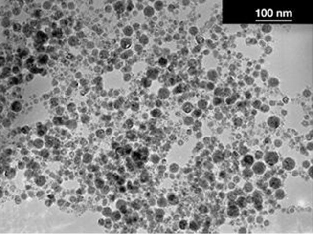
TEM Image
Source: Kyoto University Nanotechnology Total Support Project
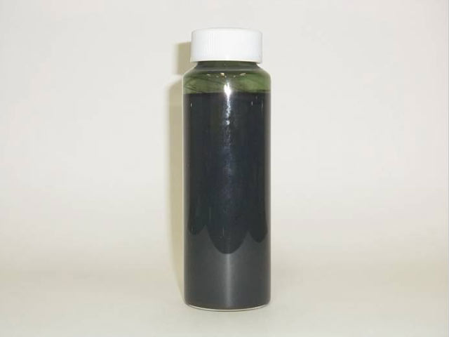
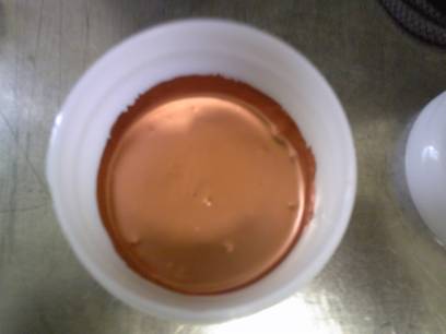
High Dispersion Concentration Copper-Based (Cu2O) Nanoparticle Ink
The ink is a high concentration dispersion of copper (I) oxide nanoparticles that is able to maintain stability for long periods.
A special manufacturing method results in particles with irregular bumpy spherical shapes and diameters distributed within a narrow range at about 50 nm. Because they form coating films easily and enable low-temperature conductor processing, they are used to form highly conductive copper coatings. The material can be applied to a wide selection of substrates and the copper coating can be soldered.
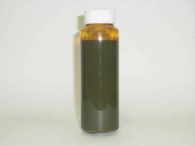
Photo of Ink
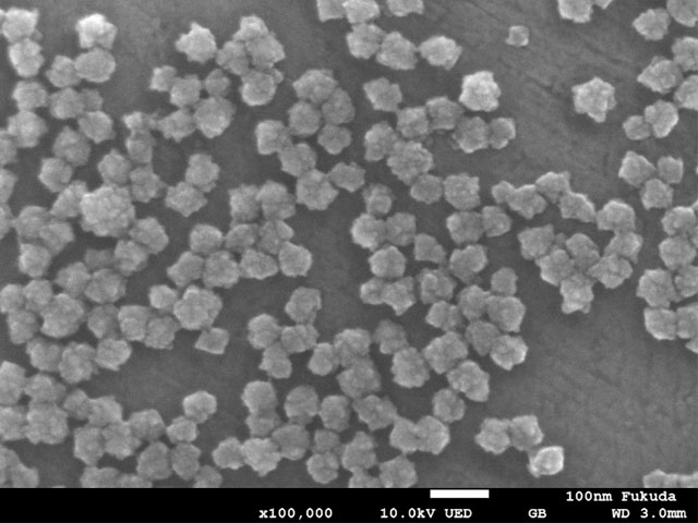
FE-SEM Image
Application Example (1)
Using Copper (I) Oxide Nanoparticle Dispersion Ink to Form Circuits on an ITO Membrane by Inkjet Printing
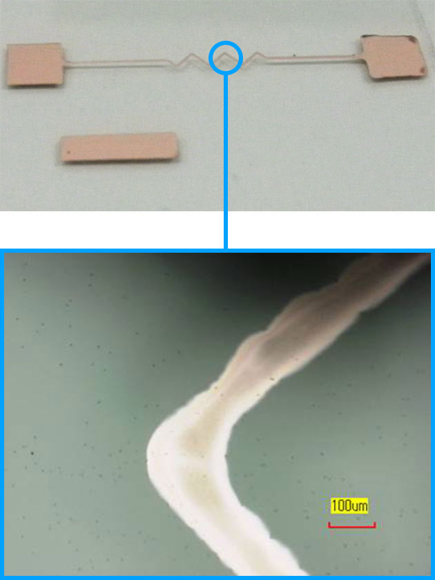
Conductor Formed by Inkjet Printing (a)
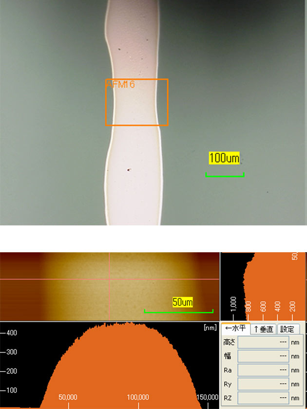
AFM Images from Linear Portion and Cross Section with Ideal Profile (b)
Application Example (2)
Hybrid Copper Paste Comprising Copper (I) Oxide Nanoparticle Dispersion Ink
Hybrid Copper Paste (a)
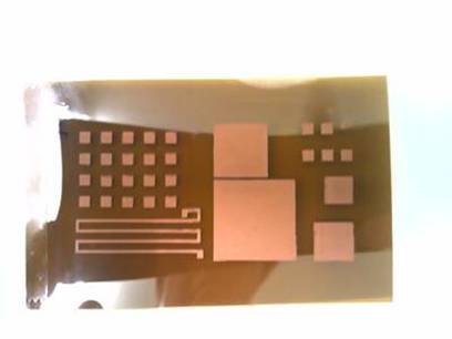
Printed Pattern Formed on Film (b)