October 25, 2021
Abstract
With the advent of the IoT era, in which all devices around the world communicate instantly via networks, the spread of 5th generation mobile communication systems (5G) is expected to respond to the rapidly increasing communication traffic.
With 5G, higher frequency bands are used, and circuit board conductors are increasingly faced with skin effect problems. In other words, it is strongly influenced by the surface condition of the copper foil used for the circuit conductor. The surface texture of copper foil has long been evaluated with a stylus type roughness meter. However, the surface roughness of copper foil for high-frequency substrates is becoming finer than the stylus radius of stylus type roughness meters in many grades. In this paper, we introduce a method for accurately evaluating the surface properties of copper foil for high-frequency circuit boards, and report on its effect on transmission characteristics.
Key Words
High Frequency PCB, Copper Foil, CLSM, Beyond 5G, millimeter-wave
Introduction
The mission of copper foil (conductors) to reduce the transmission loss required for high-frequency substrates is to reduce conductor loss. One of the important factors that govern the conductor loss of a conductor that is pure copper is the skin effect. The skin effect causes an increase in conductor loss due to the concentration of the signal on the conductor surface as the signal frequency increases. The depth at which the signal current is concentrated is called the skin depth. The surface smoothness (reduced roughness) of the copper foil is important in order for high-frequency signals to flow better through the copper foil circuit as a conductor.
As for the surface texture parameters of copper foil. Rz(DIN) or RTM indicated in IPC4562A standard is applied to the maximum height roughness, and RzJIS indicated in JPCA-UB01 standard is applied to the ten-point roughness. For these surface roughness measurements, a contour curve type "stylus type roughness meter" is used, and the tip stylus diameter is 5 μm or 2 μm.
The skin depth (δ) of the signal in the conductor for 5G communication is calculated by the formula in Figure 1, which is approximately 1.1 μm at 3 GHz in the FR1 frequency band (Sub 6 GHz band) and approximately 0.36 μm at 30 GHz in the FR2 (millimeter wave band).
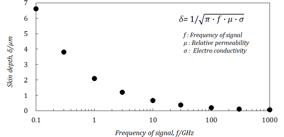
Figure 1 Skin depth plot at each frequency
Since the frequency band used in the current mainstream 4th generation mobile communication system (4G) is 700MHz to 3.5GHz, the surface roughness RzJIS of copper foil for high-frequency should be 2.5μm or less.
The profile (roughness) of copper foil is stipulated in JPCA-UB-01 as following Table 1. Most of the copper foil for high frequency will fall within the category Z.
Table 1 Classification of copper foil indicated in JPCA-UB01 standard Table 16.3-23

A stylus type roughness meter is applied as a method for measuring surface roughness. Figure 2 shows a mutual magnification schematic diagram of a copper foil cross section with a surface with a maximum height roughness Rz of 1 μm and a roughness meter with a stylus tip diameter of 2 μm.
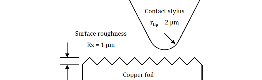
Figure 2 Mutual magnification schematic diagram of stylus type roughness meter
It is easy to see that it is not a method that can accurately trace the surface texture of copper foil for high frequency.
As a method for evaluating the surface texture of such a low-profile copper foil for high frequency, a three-dimensional method using a confocal laser scanning microscope (CLSM) is applied instead of the conventional contour curve method using a stylus. The surface texture of the three-dimensional method is defined by the ISO 25178 standard. Specific measurement conditions are determined in each industrial field because the optimum conditions differ depending on the object to be measured. For copper foil, they are specified in the JPCA-KHS01 standard.
In this paper, we show the measurement results of the surface texture of copper foil for high frequency following the JPCA-KHS01 standard, and evaluate the effect on transmission characteristics.
Evaluation equipment and conditions
First, the measurement conditions for CLSM shown in the JPCA-KHS01 standard are described. CLSM must comply with the ISO 25178-607 standard. In addition, in order to obtain sufficient optical resolution (Resolving power) for measurement, the laser light is specified as a purple laser light source represented by a wavelength of 405 nm, and the numerical aperture of the objective lens is specified as 0.95.
The optical resolution δ is calculated from Rayleigh's formula shown in Equation-1 and is 0.26 μm for the specified device.
δ = 0.61 x λ / NA (Equation-1)
λ : Wavelength of light source
NA : Numerical Aperture
The standard evaluation area is 125 μm square, which usually corresponds to a 100x objective lens. Since general CLSM collects data at 1,024 points square, the sampling data interval is 0.122 μm, which enables data sampling that exceeds the optical resolution. CLSM can narrow down the scanning range (field of view), so it is also possible to use an objective lens with a numerical aperture of 0.95 and a magnification of 50x.
Copper foil for high frequency is often used with a foil thickness of 1/2 oz or less, and it is difficult to install it as a perfect flat surface when measuring samples, and there is concern about the influence on data due to the installation shape. To exclude this disturbance, the F operation is performed as a cubic surface function approximation. Furthermore, in order to accurately detect fine irregularities that affect high-frequency signals, long-period noise is processed at 50 μm as an L filter, and low-period noise is processed at 0.5 μm as an S filter. The ISO 25178-3 standard stipulates restrictions on the data sampling interval for the S filter value, and in the above general example, a nesting index value of 0.366 μm or more, which is three times 0.122 μm, is used.
The S-L curved surface extracted in this way is evaluated with various parameters.
Surface texture parameters are defined by the ISO 25178-2 standard. In the JPCA-KHS01 standard, Section 4.2.1 indicated the test method and specification classification for the contour curve method and the three-dimensional method as the surface roughness, and RzJIS is specified for the contour curve method and Sa is specified for the three-dimensional method.
The specification classification by the three-dimensional method described in Section 4.2.1-2 of the same standard is shown in Table 2.
Table 2 Specification classification by three-dimensional method of copper foil surface roughness

Evaluation sample
The SEM image of the copper foil for high-frequency substrates used for the evaluation are shown in Figure 3, and the surface roughness (Sa, μm) and the classification in the JPCA-KHS01 standard are shown in Table 3.

Figure 3 SEM photograph of (a) Foil_1, (b) Foil_2, (c) Foil_3, (d) Foil_4
Table 3 Surface roughness and classification of copper foil

Copper foil for high-frequency substrates (Foil_1~4) are classified as the same category "Z" in the JPCA-UB01 standard, but are classified as "UA~UC" in the JPCA-KHS01 standard.
Evaluation of transmission loss
Next, the relationship between the surface roughness of the evaluation copper foil and the conductor loss was evaluated. A glass epoxy resin (FR-4) was used as the base material to keep the dielectric loss stable. The thickness of the copper foil was 1/3 oz (12 μm), and an evaluation microstrip line with a circuit length of 100 mm was manufactured for the evaluation. The equipment configuration for evaluation of transmission loss are shown in Table 4.
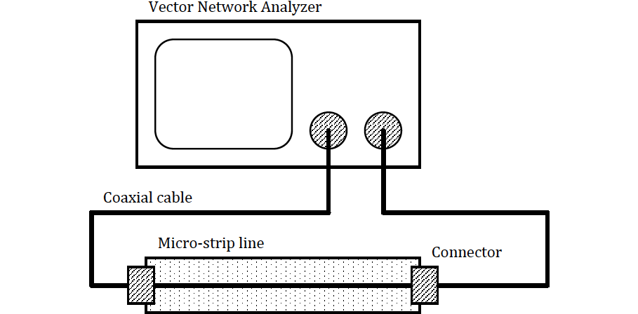
Figure 4 The equipment configuration for evaluation of transmission loss
For the microstrip line, the conductor (copper foil) circuit width was adjusted so that the characteristic impedance was 50Ω. Table 4 shows the surface roughness of copper foil for high-frequency substrates and the results of transmission loss at a frequency of 20 GHz.
Table 4 Surface roughness and transmission loss

It can be seen that transmission loss (conductor loss) is reduced for products with low surface roughness. Figure 5 shows the results of measuring the transmission loss (at a frequency of 20 GHz) for copper foil varieties with various surface roughness other than these four types.
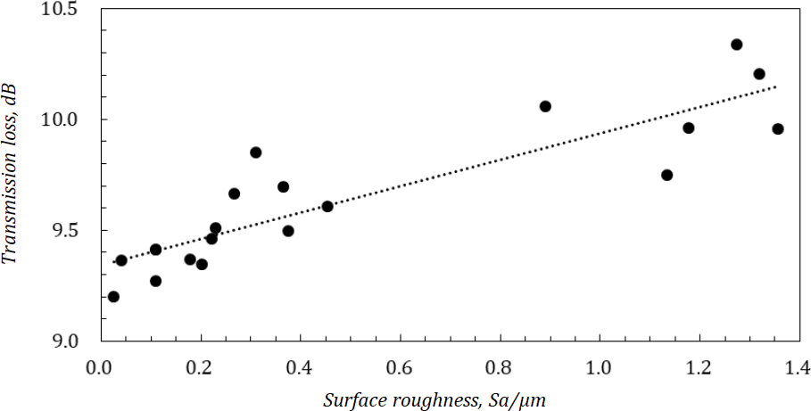
Figure 5 Relationship between surface roughness of copper foil and transmission loss
This result shows that the transmission loss (conductor loss) correlates with the surface roughness.
Summary
With 5G, higher frequency bands are used, and circuit board conductors are increasingly faced with skin effect problems. In other words, it is strongly influenced by the surface condition of the copper foil used for the circuit conductor. A variety of copper foil for high-frequency substrates with a lower roughness surface has been developed, and the specification classification is specified by the JPCA-KHS01 standard. As for the surface roughness measuring instrument, in addition to the conventional stylus type, a three-dimensional method using confocal laser scanning light is specified. This method has made it possible to more accurately capture the surface texture of copper foil for high-frequency substrates.
From the measurement results of the transmission loss using the microstrip line, it was confirmed that there is a correlation between the copper foil surface roughness Sa measured by the three-dimensional method and the transmission loss (conductor loss).
Future tasks
The factors for reducing transmission loss required for high-frequency boards can be broadly divided into two types. One is conductor loss and the other is dielectric loss. It is known that the dielectric loss depends on the permittivity of the dielectric and the dielectric loss tangent. Instead of thermosetting phenol resin and epoxy resin, which have been widely used for printed circuit boards, there are various thermoplastic resins such as liquid crystal polymer (LCP), polyphenylene ether (PPE), and fluororesin (PTFE) which are currently major materials for high frequency substrates.
As mentioned in this paper, it is necessary to reduce the surface roughness of the copper foil in order to improve the conductor loss, but in general, dielectric materials with excellent dielectric properties tend to have low adhesiveness to metals. The circuit width of printed circuit boards becomes narrower year by year, and ensures the adhesion strength between conductors (copper foil) and dielectrics is also an issue. For this reason, we consider that not only low surface roughness but also optimization of the particle shape is an issue. Specifically, the surface roughness Sa is a parameter in the height direction, but the copper foil surface has the shape of an aggregate of particles as shown in Figure 3. As shown in Figure 6, it is necessary to consider the effect of different intervals with the same height, and in the three-dimensional method, we plan to conduct a survey using the Sdr (RSAR) parameter, which represents the surface area ratio.
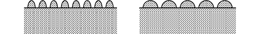
Figure 6 Difference in particle shape on the surface of copper foil
References
- ISO 25178-2:2012 Geometrical product specifications (GPS) - Surface texture: Areal - Part 2: Terms, definitions and surface texture parameters
- ISO 25178-3:2012 Geometrical product specifications (GPS) - Surface texture: Areal - Part 3: Specification operators
- ISO 25178-607:2019 Geometrical product specifications (GPS) - Surface texture: Areal - Part 607: Nominal characteristics of non-contact (confocal microscopy) instruments
- IPC-4562A - April 2008 Metal Foil for Printed Board Applications
- JPCA-UB01-2017 JPCA Standard on Electronic Circuit Boards - Edition 3 -
- JPCA-KHS01-2021 Guidelines for high-speed transmission line test methods of the flexible printed wiring board - Edition 2 -